Fewer spins
DFM and DFA applied from the first schematic, so fewer revisions before production.
6,250 boards shipped. We design boards from schematic capture to an assembled prototype. Layer count, stack-up and assembly constraints are agreed before anything goes to the fabricator.
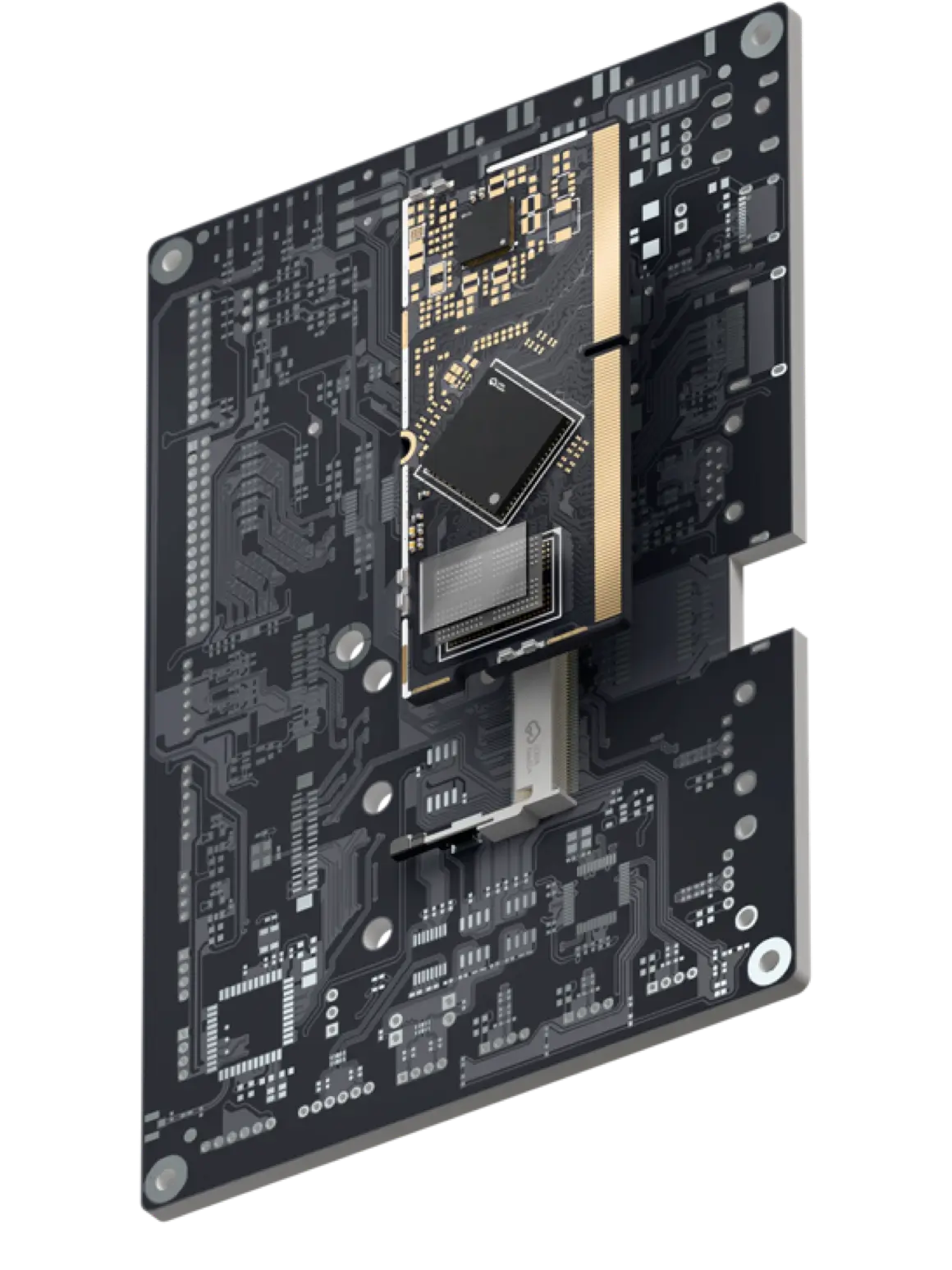
DFM and DFA applied from the first schematic, so fewer revisions before production.
We design the board and coordinate fabrication and assembly with approved partners.
Board designs and client details are never published or shared without consent.
Requirements, constraints and target volumes agreed and quoted.
Schematic, stack-up and layout, with DFM and DFA applied throughout.
Coordinated with approved fabrication and assembly partners.
Assembled boards delivered, with defects addressed within the reporting period.
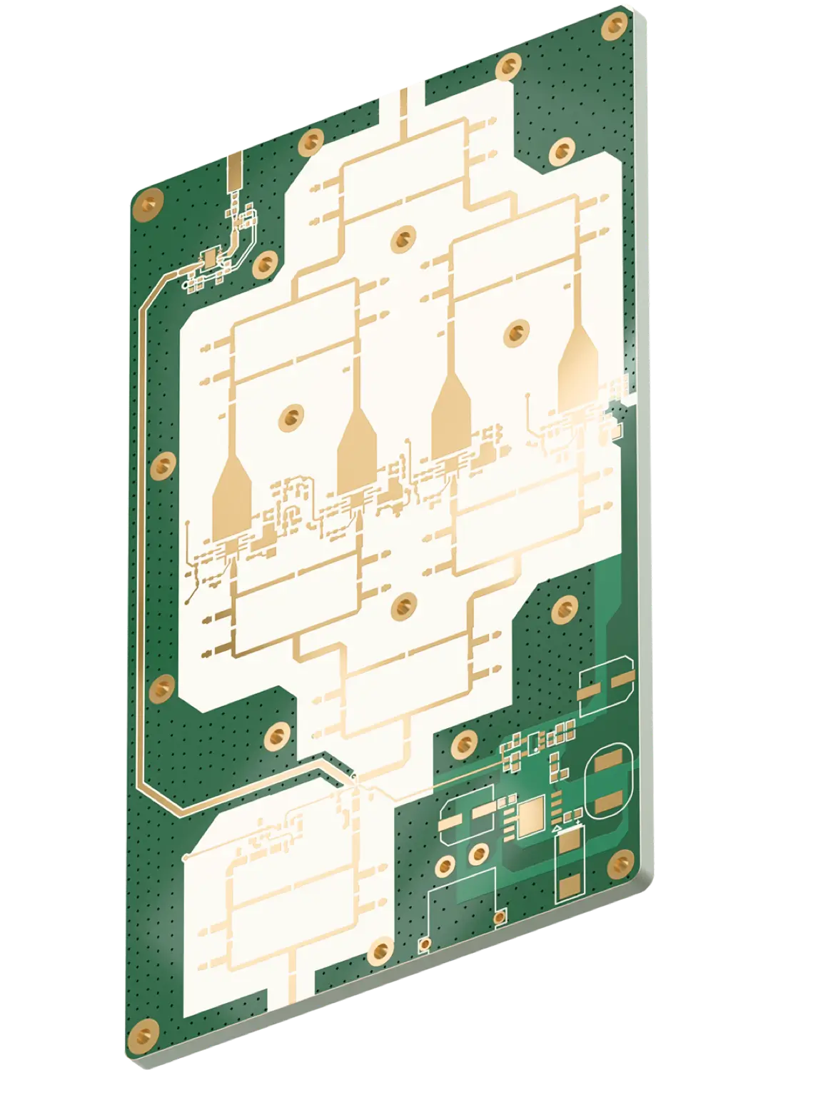
6,250
Single and multilayer boards, up to 32 layers, built through approved fabrication and assembly partners. Client designs stay confidential.
Common questions about PCB & Electronics.
No. PCB design is done in house. Fabrication and assembly are carried out through approved manufacturing and assembly partners. We coordinate that process and remain responsible for manufacturing defects reported within the defect-reporting period.
Board designs stay confidential and are not published without the client's consent. We are happy to talk through comparable work directly: layer counts, stack-ups, the manufacturing constraints involved and how a board was taken to production.